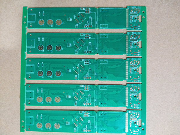
What is the structure of blind buried hole circuit board?
Blind buried-hole circuit boards have the characteristics of free zigzag, folding and winding, free movement and expansion in three-dimensional space, good heat dissipation performance and high precision, lightweight, miniaturization and thinning, so as to achieve the integration of components and wires. Next, we will understand its structure and appearance treatment.
Structure:
Blind buried-hole PCB mainly contains blind holes and buried holes. Blind holes refer to the top and bottom surfaces of PCB, which have a certain depth. They are used to connect the surface circuit and the underlying inner circuit. The depth of the holes and the aperture generally do not exceed a certain ratio. Buried holes refer to the connecting holes located in the inner layer of PCB, which will not extend. To the appearance of the circuit board.
Appearance processing:
Blind buried-hole PCB surface treatment refers to the treatment of dirt and sundries on the surface of Blind buried-hole PCB. Generally, PCB surface treatment in PCB factory is divided into two processes, one is post-drilling treatment and the other is final treatment.

After-treatment of drilling: Because the copper foil from the drill bit will appear on the circuit board after drilling, the circuit board must be treated after drilling. The treatment method is to clean the oxide layer of the circuit board and the copper wire caused by drilling directly by brushing machine. This step is very important. If the oxide layer is not removed, the adhesion of the resistance to welding will be greatly reduced by screen printing, which will lead to the drop of the resistance. If the copper wire is to be treated cleanly, when it is lightly printed and soldered, it will lead to the residual copper wire on the circuit board, which will break the screen if the appearance of the circuit board is not good.
Blind buried hole PCB appearance final treatment: PCB final treatment depends on the PCB pad is what treatment, if it is rosin treatment, then the surface treatment should be clean before the pad treatment after rolling rosin. If it is tin spraying treatment, then the printed circuit board should be sprayed tin first and then cleaned by the brusher. If it is anti-oxidation treatment, the treatment method and roll-coating rosin are much the same. The final treatment of blind buried-hole PCB is also very important. If the PCB pad is not treated properly, the residue will be left, which will lead to the phenomenon of virtual welding or poor welding when the PCB is welded.
Nowadays, with the rapid development of information industry, some electronic products such as mobile phones and computers are inseparable from the use of blind buried-hole circuit boards, which are widely used. Although the blind buried-hole circuit boards are small and insignificant, they can play a vital role.
The article originated from Jiangmen single-sided and double-sided circuit boards. http://m.jzfwq.com
-
07-18
What is the structure of blind buried hole circuit board?
Blind buried-hole circuit boards have the characteristics of free zigzag, folding and winding, free movement and expansion in three-dimensional space, good heat dissipation performance and high precis
-
07-18
What role does copper play in circuit boards?
PCB manufacturers take you to know that there are several reasons for PCB copper laying: 1. EMC can shield large area of ground or power supply copper, and some special areas, such as PGND, play a pr
-
07-18
Four matters needing attention in choosing PCB manufacturer
When choosing PCB manufacturers, the price of PCB manufactured by professional manufacturers will be more affordable, and the quality assurance will be stronger, which will be more guaranteed after
-
07-18
How to use three glue-proof PCB correctly?
Sanfang gum does not contain evaporative substances such as acetone and xylene, which is more environmentally friendly and safe. Mainly used in electronic circuits and components to form a protectiv